
 Ammar Sabilarrohman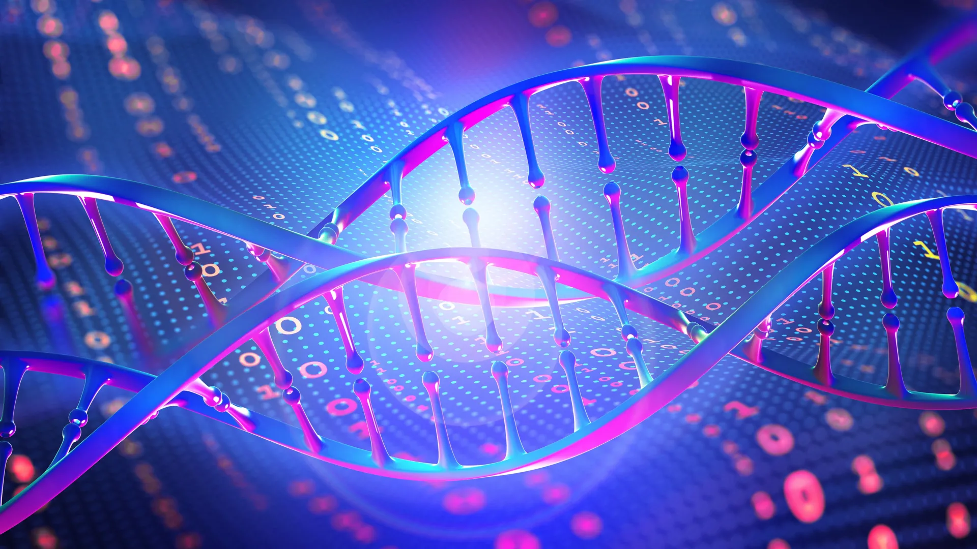
In the grand architecture of life, DNA serves as the ultimate storage medium—a dense, elegant, and durable blueprint capable of encoding the complexities of entire organisms within microscopic structures. For decades, computer scientists have looked at the double helix with envy, recognizing that a single gram of the molecule could theoretically hold upwards of 215 million gigabytes of data.
For years, however, the "biological" and the "electronic" remained fundamentally estranged. DNA is soft, aqueous, and complex; silicon is rigid, dry, and standardized. Bridging this chasm has been the "holy grail" of materials science. Now, a team of researchers at Penn State University has effectively broken this barrier. By synthesizing custom DNA sequences and integrating them with crystalline perovskite semiconductors, the team has engineered a bio-hybrid memristor that functions with unprecedented efficiency, potentially ushering in a new era of brain-inspired, low-power computing.
The Convergence of Biology and Electronics
The breakthrough, published in the journal Advanced Functional Materials, represents a fundamental shift in how we conceive of hardware. The researchers have moved beyond the traditional reliance on rigid silicon-only architectures, turning instead to a hybrid platform that leverages the structural precision of synthetic DNA.
The device is built upon two core pillars:
- Synthetic DNA: Unlike natural DNA, which is long, tangled, and biologically unpredictable, the team utilizes short, rigid, and programmable genetic sequences. These are chemically engineered to meet precise electronic specifications.
- Crystalline Perovskite: A class of materials widely recognized for its superior optoelectronic properties in solar cells and high-speed data storage.
"Biology and electronics are different domains," explains Kavya S. Keremane, a postdoctoral researcher in materials science and engineering at Penn State and a co-corresponding author of the study. "Bridging these two fields required developing an entirely new materials platform that allows them to function seamlessly together. By combining the information storage capabilities of DNA with the exceptional electronic properties of perovskite semiconductors, we created a bio-hybrid system that fundamentally changes how low-power memory devices can be designed."
Chronology of the Innovation: From Concept to Circuit
The road to this bio-hybrid memristor began with a fundamental question: How can we make biological molecules behave like conductors?
The Preliminary Phase: The team first recognized that natural DNA’s messy, "wet spaghetti" structure was a non-starter for high-precision electronics. The research trajectory shifted toward synthetic biology, where the ability to computationally determine the exact length and composition of a DNA strand allowed for the creation of structured, predictable nanomaterials.
The Doping Breakthrough: The most critical technical milestone involved "doping." By integrating silver nanoparticles into the layers of customized DNA sequences, the researchers transformed the DNA from an insulator into a conductive pathway. This doping process not only facilitated the flow of electrons but also forced the molecular units of the DNA to align in a highly ordered, crystalline-like arrangement.
Integration and Testing: Once the DNA-silver complex was successfully synthesized, it was integrated with thin films of perovskite. The team then subjected the resulting device to rigorous electrical testing. They found that the device exhibited "memristive" properties—meaning it could "remember" the direction of a current flow even after the power was disconnected. Crucially, it did so while operating at voltages lower than 0.1 volts, a stark contrast to the energy-intensive requirements of current-generation flash memory.
Supporting Data: Efficiency and Stability Metrics
The performance metrics of the new memristor are striking, particularly when measured against the constraints of current artificial intelligence (AI) hardware. As AI models grow in complexity, the "memory wall"—the energy cost of moving data between memory and processing units—has become a significant bottleneck.
- Energy Efficiency: The bio-hybrid device consumes 100 times less power than traditional storage technologies like flash drives. In head-to-head functional tests, the device performed identical memory tasks while consuming only one-tenth the power of comparable existing technologies.
- Thermal Stability: One of the traditional weaknesses of perovskite-based devices is their sensitivity to heat. However, the DNA-enhanced version proved remarkably robust, maintaining consistent operational integrity at temperatures as high as 250 degrees Fahrenheit.
- Longevity: In shelf-life testing, the devices remained functional at room temperature for more than six weeks without degradation, a performance milestone that significantly outperforms previous perovskite-based memory storage experiments.
"Using just the DNA or just perovskite alone did not produce near as robust a result as the combination," says Keremane. "It’s this combination that enables a very high memory storage density that requires very little power."
Official Perspectives on Neuromorphic Computing
The implications of this research extend far beyond mere data storage. As the global economy pivots toward AI-driven technologies, the demand for "neuromorphic computing"—systems designed to mimic the neural pathways of the human brain—has reached a fever pitch.
Bed Poudel, a research professor of materials science and engineering and co-corresponding author, emphasizes the strategic necessity of this research. "As the demand for artificial intelligence grows, we need a new strategy for low-power, high-storage devices," Poudel notes.
Neuromorphic systems operate by evaluating multiple inputs simultaneously and making decisions based on weighted historical data, much like human synapses. Traditional silicon architecture struggles to do this efficiently because it separates memory (RAM/Hard Drive) from processing (CPU/GPU). The Penn State team’s memristor, however, stores and processes information in the same physical space.
"Nature has the solution—we just have to find it and apply it," Poudel adds. "This work of integrating DNA into electronics to do amazing things gives a glimpse into what is possible."
Neela H. Yennawar, director of the Penn State Huck Institutes of the Life Sciences’ Biomolecular Interactions Core Facility, highlights the modular nature of the design. "We can computationally determine exactly which sequences we need and how long they should be, and then we can rationally design them with synthetic DNA," she says. "These structures can be systematically doped with silver and other ions and engineered to interface seamlessly with perovskites—transforming DNA from a biological macromolecule into a programmable, multifunctional nanomaterials platform."
Implications for the Future of Tech
The successful marriage of synthetic biology and semiconductor physics opens several doors for the future of the digital landscape:
1. Scaling AI Infrastructure
As large language models and neural networks grow, the energy footprint of data centers has become a major environmental and economic concern. A memristor that functions at a fraction of the power could potentially shrink the power requirements of AI training clusters, making them more sustainable and economically viable.
2. High-Density Archival Storage
While this research focuses on active memory (memristors), the foundational technology proves that DNA can be effectively "wired" into electronic systems. This suggests a future where DNA-based storage, currently relegated to slow, cold-storage archival, could become a part of the active memory hierarchy in high-performance devices.
3. Bio-Integrated Electronics
The biocompatibility of DNA suggests that this platform could eventually serve as the interface for brain-computer interfaces (BCIs) or advanced medical sensors that need to communicate directly with human cells without triggering immune responses or causing toxic accumulation.
Conclusion and Collaborative Scope
The research, which has already been the subject of a patent application, is the result of a multi-institutional effort. In addition to the lead team at Penn State, researchers from the University of Minnesota, including Rashmi Jha and Abhinav Gorthy, provided critical expertise. The project was supported by the U.S. National Science Foundation and the National Institutes of Health, underscoring the interdisciplinary importance of the work.
As the team looks toward the future, the focus will shift from the laboratory proof-of-concept to scaling the manufacturing processes. The challenge will be to ensure that the "rational design" of synthetic DNA can be reproduced at the scale of billions of transistors—the standard for modern computer chips.
If this technology can be scaled, the implications are profound. We are witnessing the birth of a "biological transistor," a device that doesn’t just calculate with cold, hard logic, but does so with the elegant, high-density efficiency that life has been perfecting for billions of years. In the fusion of the double helix and the perovskite crystal, the future of computing may finally be finding its way home.


 Dwi Wanna

 Muslim
 Nana Wu

 Rifan Muazin
 Asro
Asro