
 Laily UPN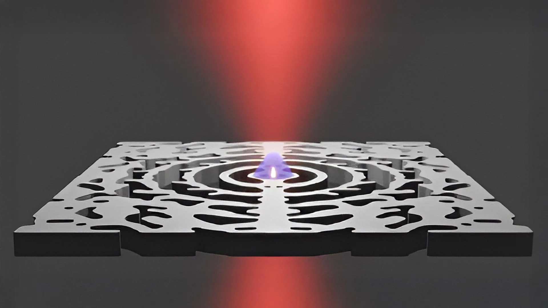
The landscape of modern computing is approaching a physical "brick wall." For decades, the industry has followed Moore’s Law, packing ever-increasing numbers of transistors onto silicon microchips. However, as these components shrink to the atomic scale, the reliance on copper wires to move data via electrical signals has become a primary bottleneck. The heat generated by electrical resistance and the inherent speed limitations of electrons are now stifling innovation.
A team of researchers at the Technical University of Denmark (DTU) may have just provided the architectural blueprint to overcome this barrier. In a breakthrough study recently published in the scientific journal Science Advances, the team unveiled a novel nanolaser capable of bringing optical communication directly onto the microchip. By shifting from electrons to photons, this technology promises to usher in an era of faster, cooler, and significantly more energy-efficient digital devices.
The Core Innovation: Breaking the Size Barrier
At the heart of the DTU discovery is a fundamental shift in how light is manipulated. Traditionally, lasers are bulky, complex systems. Even "miniature" lasers used in current telecommunications hardware are massive compared to the nanometer-scale transistors found on modern microprocessors. The challenge has always been the "diffraction limit"—a physical constraint that dictates how small a laser cavity can be while still trapping and amplifying light.
The Science of the Nanocavity
The DTU team, led by Professor Jesper Mørk alongside Drs. Meng Xiong and Yi Yu, successfully engineered a structure known as a "nanocavity." Developed in collaboration with Professor Ole Sigmund’s group at DTU Construct, this structure is designed to trap and concentrate light within an exceptionally confined, microscopic region.
By utilizing advanced nanofabrication techniques within DTU’s state-of-the-art Nanolab, the researchers created a device where both photons and electrons are squeezed into the same tiny volume. This precise spatial overlap allows the laser to achieve high-intensity light emission at room temperature while requiring only a fraction of the energy traditionally needed to stimulate such a reaction.
This accomplishment effectively shatters the conventional limits regarding the minimum size of a functional laser. It is not merely a smaller laser; it is a fundamental reconfiguration of light-matter interaction at the nanoscale.
Chronology: From Fiber Optics to Chip-Level Photonics
To understand the magnitude of this breakthrough, one must look at the historical trajectory of data transmission.
- The 1980s–1990s (The Fiber Optic Age): The telecommunications industry revolutionized global connectivity by switching from copper cables to fiber optics. By using light to transmit data, researchers realized they could move information across oceans at the speed of light with minimal signal loss.
- The 2000s–2010s (The Bottleneck): While the internet backbone became optical, the "last mile"—the path from the server rack to the individual processor—remained stubbornly electrical. Inside the computer, data still moves via electrons, creating the "heat wall" that limits processor clock speeds.
- 2020–2023 (The Search for On-Chip Integration): The global research community shifted focus toward "Silicon Photonics." The goal was to place lasers directly onto silicon chips. However, previous attempts were either too large to integrate in high densities or required cryogenic cooling to function.
- 2024 (The DTU Breakthrough): The team at DTU successfully demonstrated a stable, energy-efficient nanolaser that operates at room temperature, providing a viable pathway for mass-integrating thousands of these units onto a single chip.
Supporting Data: The Case for Efficiency
The primary incentive for the shift to photonics is not just speed, but thermodynamic efficiency. Current high-performance computing (HPC) environments, such as those powering modern AI models, are constrained by the sheer amount of electricity required to cool the hardware.
Energy Consumption Metrics
According to Professor Jesper Mørk, the integration of nanolasers into computer architecture could reduce energy consumption by up to 50%. This projection is based on the following factors:
- Reduced Resistance: Moving electrons through copper wires creates heat (Joule heating). Photons, which have no charge, do not experience resistance as they travel, leading to near-zero energy loss during transmission.
- Higher Bandwidth Density: Photonic signals do not suffer from the same electromagnetic interference as electrical signals, allowing for significantly higher data throughput in smaller spaces.
- Lower Thermal Overhead: Because the system generates less heat, the infrastructure required for cooling—often a massive portion of a data center’s power budget—can be drastically scaled down.
The potential for "thousands of lasers" on a single chip means that future processors could communicate with internal memory and external networks at speeds currently unattainable, all while remaining within the thermal limits of modern consumer hardware.
Official Perspectives: The Path Forward
The researchers involved in the project emphasize that this is a "first step" toward a long-term goal, but they remain optimistic about the timeline.
"The nanolaser opens up the possibility of creating a new generation of components that combine high performance with minimal size," says Professor Mørk. "This could be in information technology, where ultra-small and energy-efficient lasers reduce energy consumption, or in the development of sensors for the healthcare sector, where the nanolaser’s extreme light concentration can deliver high-resolution images and ultrasensitive biosensors."
The next major milestone is the transition from an optical-pumped system to an electrically driven system. Currently, the laser is stimulated by an external light beam. To be useful in a commercial smartphone or data center chip, the laser must be integrated into the electrical circuit of the chip itself, drawing power directly from the device’s battery or power supply.
Mørk’s team estimates that solving these remaining technical hurdles—specifically electrical injection—will take approximately 5 to 10 years.
Implications: A New Era of Technology
The impact of this technology extends far beyond faster gaming PCs or smartphones.
1. Data Centers and the Climate
Data centers are currently among the largest consumers of electricity globally. As the world moves toward an AI-driven economy, the energy demand for data processing is skyrocketing. If the DTU nanolaser can cut energy consumption by 50% across these facilities, the environmental impact would be significant, potentially shaving gigatons of CO2 emissions off the global digital carbon footprint.
2. Healthcare and Biosensing
The ability to concentrate light into such a small volume has profound implications for diagnostics. The researchers noted that this technology could be the foundation for "ultrasensitive biosensors." These sensors could be integrated into lab-on-a-chip devices, capable of detecting diseases, viruses, or chemical markers at the single-molecule level. Because the laser is so compact, these diagnostic tools could be portable, bringing hospital-grade precision to remote or resource-limited environments.
3. The Future of Computing Architecture
If photonics replaces electrons for data transmission, the very shape of the computer chip will change. We might see the rise of "optically connected" processors where communication latency between the CPU, RAM, and storage is essentially eliminated. This would not only make devices faster but would allow for entirely new forms of parallel computing that are currently bottlenecked by the time it takes for data to physically move between components.
Conclusion: The Horizon
The breakthrough at DTU is a testament to the power of interdisciplinary research. By bridging the gap between nanotechnology, optics, and computer engineering, the researchers have laid the groundwork for a transition that many thought was decades away.
While the "optical chip" is not yet available for mass production, the successful demonstration of the nanolaser proves that the physics are sound. As the team moves toward electrical integration, the focus will shift from fundamental research to industrial scalability.
We are standing at the threshold of a technological evolution. Just as the vacuum tube gave way to the transistor, the electronic microchip may soon give way to the photonic microchip. If the next decade of development mirrors the success of this recent publication, the computers of the 2030s will be faster, smarter, and more efficient than we ever dared to imagine—powered, quite literally, by light.


 Nila Kartika Wati
 Nana Wu
 Basiran
 Neng Nana
 Iffa Jayyana
 Raul Delapena Setiawan
 Rifan Muazin
 Asro
Asro